- 您现在的位置:买卖IC网 > Sheet目录2010 > MAX5237EUB+ (Maxim Integrated Products)IC DAC 10BIT DUAL 5V 10-UMAX
MAX5236/MAX5237
Detailed Description
The MAX5236/MAX5237 10-bit, voltage-output DACs
are
easily
configured
with
a
3-wire
SPI/
QSPI/MICROWIRE serial interface. The devices include
a 16-bit data-in/data-out shift register and have an input
consisting of an input register and a DAC register. In
addition, these devices employ precision trimmed inter-
nal resistors to produce a gain of 1.6384V/V, maximiz-
ing the output voltage swing, and a programmable
shutdown output impedance of 1k
or 200k. The full-
scale output voltage is 4.092V for the MAX5237 and
2.046V for the MAX5236. These devices produce a
weighted output voltage proportional to the digital input
code with an inverted rail-to-rail ladder network (Figure 3).
External Reference
The reference inputs accept both AC and DC values
with a voltage range extending from 0.25V to 2.6V for
the MAX5237 and 0.25V to 1.5V for the MAX5236. For
proper operation do not exceed the input voltage
range limits. Determine the output voltage using the fol-
lowing equation:
VOUT_ = (VREF_ x NB / 1024) x 1.6384V/V
where NB is the numeric value of the DACs binary input
code (0 to 1023), VREF_ is the reference voltage, and
1.6384V/V is the gain of the internal output amplifier.
The code-dependent reference input impedance
ranges from a minimum of 28k
to several G at code
0. The code-dependent reference input capacitance is
typically 23pF.
Output Amplifier
The output amplifiers have internal resistors that pro-
vide for a gain of 1.6384V/V. These trimmed resistors
minimize gain error. The output amplifiers have a typical
slew rate of 0.6V/s and settle to 1/2LSB within 10s
(typ) with a load of 5k
in parallel with 100pF. Use the
serial interface to set the shutdown output impedance
of the amplifiers to 1k
or 200k.
Single-Supply 3V/5V, Voltage-Output, Dual,
Precision 10-Bit DACs
10
______________________________________________________________________________________
Pin Description
PIN
NAME
FUNCTION
1
OUTA
DAC A Output
2
REFA
Reference for DAC A
3
GND
Ground
4
LDAC
Load DACs A and B
5
CS
Chip Select Input
6
SCLK
Shift Register Serial Clock Input
7
DIN
Serial Data Input
8VDD
Positive Supply
9
REFB
Reference for DAC B
10
OUTB
DAC B Output
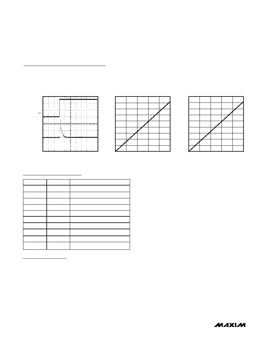
2
s/div
MAX5237
MAJOR CARRY GLITCH
CS
2V/div
MAX5236/7 toc28
OUT_
50mV/div
AC-COUPLED
0
0.50
0.25
1.25
1.00
0.75
2.00
1.75
1.50
2.25
0
0.50
0.25
0.75
1.00
1.25
MAX5236
FULL-SCALE OUTPUT VOLTAGE
vs. REFERENCE VOLTAGE
MAX5236/7
toc29
VREF (V)
V
OUT
(V)
0
1.0
0.5
2.5
2.0
1.5
4.0
3.5
3.0
4.5
0
1.0
0.5
1.5
2.0
2.5
MAX5237
FULL-SCALE OUTPUT VOLTAGE
vs. REFERENCE VOLTAGE
MAX5236/7
toc30
VREF (V)
V
OUT
(V)
Typical Operating Characteristics (continued)
(VDD = +5V (MAX5237) VDD = +3V (MAX5236), RL = 5k
, CL = 100pF, VREF = +1.25V (MAX5236), VREF = +2.5V (MAX5237), CREF
= 0.1F ceramic || 2.2F electrolytic, both DACs on, VOUT = full scale, TA = +25°C, unless otherwise noted.)
发布紧急采购,3分钟左右您将得到回复。
相关PDF资料
MAX5253AEAP+
IC DAC 12BIT QUAD 3V 20-SSOP
MAX5258EEE+T
IC DAC 8BIT OCTAL 5V 16-QSOP
MAX525AEAP+
IC DAC 12BIT QUAD LP 20-SSOP
MAX526DENG+
IC DAC 12BIT QUAD CALIB 24-DIP
MAX5302EUA+T
IC DAC 12BIT LP SERIAL 8-UMAX
MAX5304EUA+T
IC DAC 10BIT LP VOLT OUT 8-UMAX
MAX5307EUE+
IC DAC 12BIT OCT LP SER 16-TSSOP
MAX5312EAE+T
IC DAC 12BIT 5V/10V SER 16-SSOP
相关代理商/技术参数
MAX5237EUB+T
功能描述:数模转换器- DAC 10-Bit 2Ch Precision DAC RoHS:否 制造商:Texas Instruments 转换器数量:1 DAC 输出端数量:1 转换速率:2 MSPs 分辨率:16 bit 接口类型:QSPI, SPI, Serial (3-Wire, Microwire) 稳定时间:1 us 最大工作温度:+ 85 C 安装风格:SMD/SMT 封装 / 箱体:SOIC-14 封装:Tube
MAX5237EUB-T
功能描述:数模转换器- DAC RoHS:否 制造商:Texas Instruments 转换器数量:1 DAC 输出端数量:1 转换速率:2 MSPs 分辨率:16 bit 接口类型:QSPI, SPI, Serial (3-Wire, Microwire) 稳定时间:1 us 最大工作温度:+ 85 C 安装风格:SMD/SMT 封装 / 箱体:SOIC-14 封装:Tube
MAX5250ACAP
功能描述:数模转换器- DAC RoHS:否 制造商:Texas Instruments 转换器数量:1 DAC 输出端数量:1 转换速率:2 MSPs 分辨率:16 bit 接口类型:QSPI, SPI, Serial (3-Wire, Microwire) 稳定时间:1 us 最大工作温度:+ 85 C 安装风格:SMD/SMT 封装 / 箱体:SOIC-14 封装:Tube
MAX5250ACAP+
功能描述:数模转换器- DAC 10-Bit 4Ch Precision DAC RoHS:否 制造商:Texas Instruments 转换器数量:1 DAC 输出端数量:1 转换速率:2 MSPs 分辨率:16 bit 接口类型:QSPI, SPI, Serial (3-Wire, Microwire) 稳定时间:1 us 最大工作温度:+ 85 C 安装风格:SMD/SMT 封装 / 箱体:SOIC-14 封装:Tube
MAX5250ACAP+T
功能描述:数模转换器- DAC 10-Bit 4Ch Precision DAC RoHS:否 制造商:Texas Instruments 转换器数量:1 DAC 输出端数量:1 转换速率:2 MSPs 分辨率:16 bit 接口类型:QSPI, SPI, Serial (3-Wire, Microwire) 稳定时间:1 us 最大工作温度:+ 85 C 安装风格:SMD/SMT 封装 / 箱体:SOIC-14 封装:Tube
MAX5250ACAP-T
功能描述:数模转换器- DAC RoHS:否 制造商:Texas Instruments 转换器数量:1 DAC 输出端数量:1 转换速率:2 MSPs 分辨率:16 bit 接口类型:QSPI, SPI, Serial (3-Wire, Microwire) 稳定时间:1 us 最大工作温度:+ 85 C 安装风格:SMD/SMT 封装 / 箱体:SOIC-14 封装:Tube
MAX5250ACPP
功能描述:数模转换器- DAC RoHS:否 制造商:Texas Instruments 转换器数量:1 DAC 输出端数量:1 转换速率:2 MSPs 分辨率:16 bit 接口类型:QSPI, SPI, Serial (3-Wire, Microwire) 稳定时间:1 us 最大工作温度:+ 85 C 安装风格:SMD/SMT 封装 / 箱体:SOIC-14 封装:Tube
MAX5250ACPP+
功能描述:数模转换器- DAC 10-Bit 4Ch Precision DAC RoHS:否 制造商:Texas Instruments 转换器数量:1 DAC 输出端数量:1 转换速率:2 MSPs 分辨率:16 bit 接口类型:QSPI, SPI, Serial (3-Wire, Microwire) 稳定时间:1 us 最大工作温度:+ 85 C 安装风格:SMD/SMT 封装 / 箱体:SOIC-14 封装:Tube